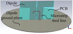
Crossed Dipole
설계자: 남보한(2014)
1. Single dipole design 1
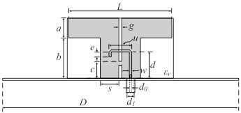
1.1 Geometry and dimensions:
Substrate:
er = 3.5, tand = 0.0018, h = 0.79mm

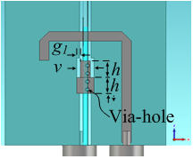
|
Design 1 |
|
|
Parameters |
Value [mm] |
|
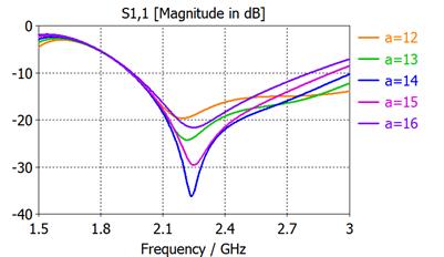
a |
14 |
|
b |
28.55 |
|
c |
10.65 |
|
d |
18.5 |
|
e |
5.2 |
|
g |
2.6 |
|
L |
72.3 |
|
s |
23 |
|
h |
w+w/2 (2.5) |
|
w |
1.67 |
|
w0 |
1.67 |
|
w1 |
3.04 |
|
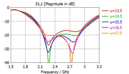
u |
15.5 |
|
v |
3 |
|
D |
150 |
|
Design 2 |
|
|
Parameters |
Value [mm] |
|
a |
14 |
|
b |
28.5 |
|
c |
12 |
|
d |
18.5 |
|
e |
5.1 |
|
g |
2 |
|
L |
71 |
|
s |
13 |
|
h |
w+w/2 (2.5) |
|
w |
1.67 |
|
w0 |
1.67 |
|
w1 |
3.04 |
|
u |
|
|
v |
|
|
D |
150 |
|
Design 3 |
|
|
Parameters |
Value [mm] |
|
a |
14 |
|
b |
28.5 |
|
c |
12 |
|
d |
18.5 |
|
e |
5.1 |
|
g |
2 |
|
L |
72 |
|
s |
13 |
|
h |
w+w/2
(2.5) |
|
w |
1.67 |
|
w0 |
1.67 |
|
w1 |
3.04 |
|
u |
16 |
|
v |
3 |
|
D |
150 |
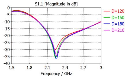
1.2 Results
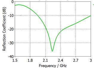
Reflection
coefficient. At 2.05-2.85GHz(33%), |S11|
< -20dB
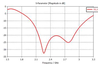
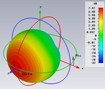
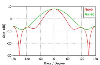
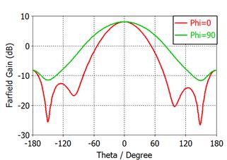
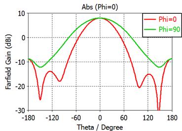
Radiation pattern. Asymmetry in the gain pattern leads to
high axial ratios at large angles. Peak gain = 8dB
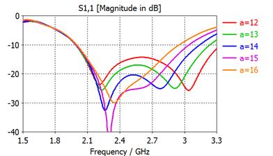
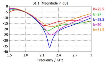
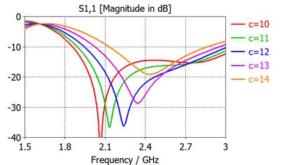
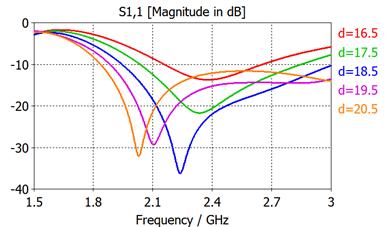
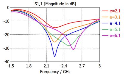
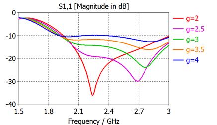
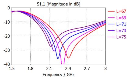
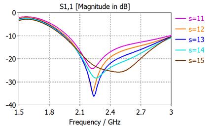
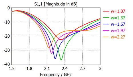
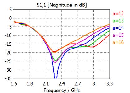
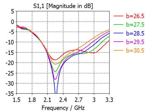
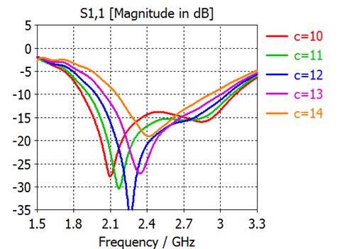
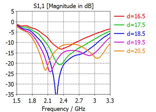
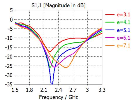
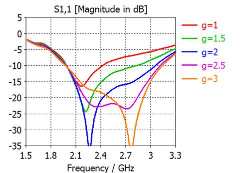
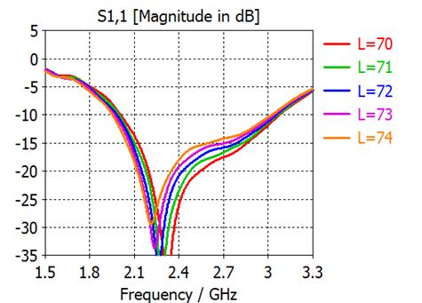
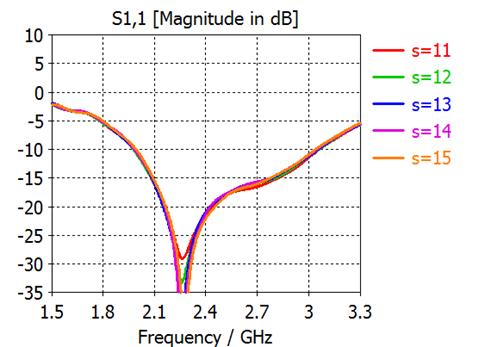
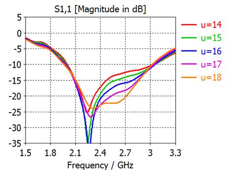
1.3 Parameter study
- Dipole
width: Controls the bandwidth
- Dipole height: Wrong figure
xxxxxx
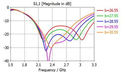
Short circuit position: Affects the bandwidth and impedance
matching
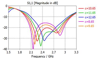
- Feeding point: Affects the impedance matching and bandwidth
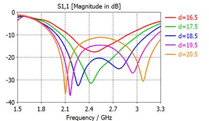
- Feed line open stub length: Mildly affects the impedance
matching.
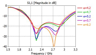
- Dipole gap: Mildly affects the impedance matching.
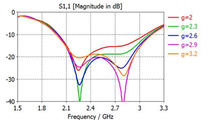
- Dipole length: Affects the range of operating
frequency and impedance matching
xxxx wrong results
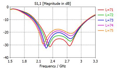
- Dipole supporting strip width: Not sensitive
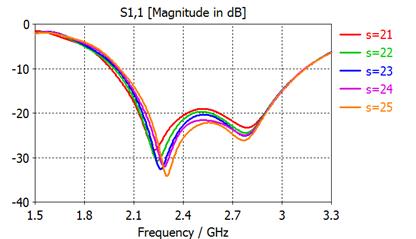
- Feed horizontal length: Not senstive
2. Single dipole design 2
|
Design
2 |
|
|
Parameters |
Value
[mm] |
|
a |
14 |
|
b |
28.5 |
|
c |
12 |
|
d |
18.5 |
|
e |
5.1 |
|
g |
2 |
|
L |
71 |
|
s |
13 |
|
h |
w+w/2 (2.5) |
|
w |
1.67 |
|
w0 |
1.67 |
|
W1 |
3.04 |
|
D |
150 |
3. Design
3
|
Design
3 |
|
|
Parameters |
Value
[mm] |
|
a |
14 |
|
b |
28.5 |
|
c |
12 |
|
d |
18.5 |
|
e |
5.1 |
|
g |
2 |
|
L |
72 |
|
s |
13 |
|
h |
w+w/2
(2.5) |
|
w |
1.67 |
|
w0 |
1.67 |
|
w1 |
3.04 |
|
u |
16 |
|
v |
3 |
|
D |
150 |
Conclusions: optimum values
a = 12-14, b= 27-30, c = 10-12, d = 19-20, e = 6-7, g = 2-3,
u = 14-18, s = 15
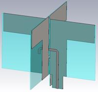
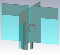
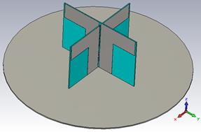
[Crossed Dipole]
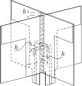
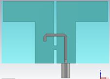
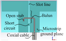
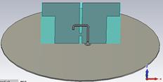
1. Design 3
ㅇ Geometry and dimensions
- Design idea:
Optimize the singla element → Apply it to the design of
the crossed dipole.
When the short circuit position is same for fabrication
purpose, the reflection coefficients are good at different frequencies.
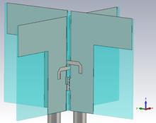
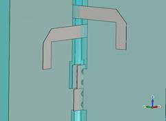
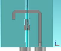
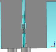
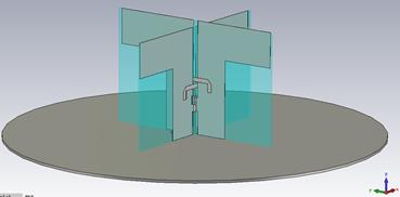
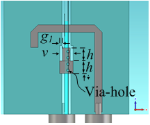
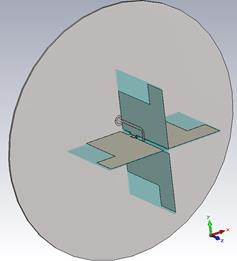
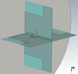
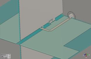
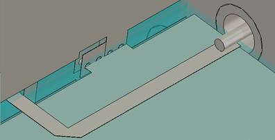
Add a
plane view of each dipole showing the slot to be removed for crossing.
|
Parameters |
Value
[mm] |
|
a |
14 |
|
b |
28.5 |
|
c |
12 |
|
d |
18.5 |
|
e |
5.1 |
|
g |
2 |
|
L |
72 |
|
s |
13 |
|
h |
w+w/2 (2.5) |
|
w |
1.67 |
|
w0 |
1.67 |
|
w1 |
3.04 |
|
u |
16 |
|
v |
3 |
|
D |
150 |
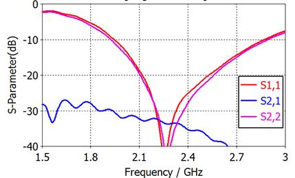
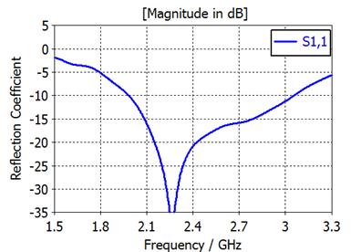
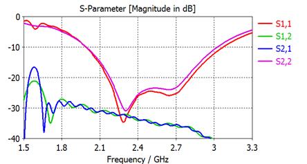
ㅇ Results
Reflection
coefficient: |S11| <
-20dB, |S21| < -31dB
over 2.15-2.75GHz
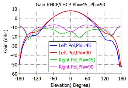
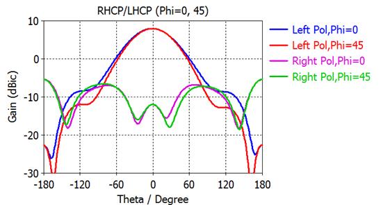
RHCP/
LHCP Pattern @2.15 Phi=45, Phi=0
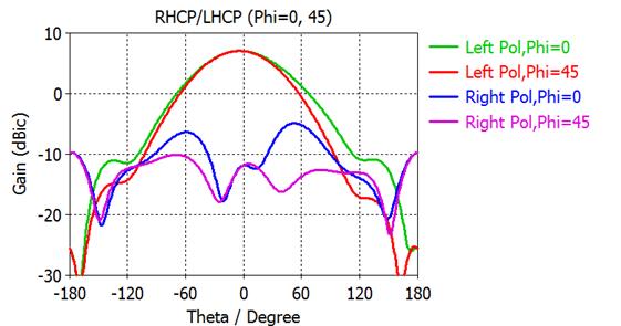
RHCP/
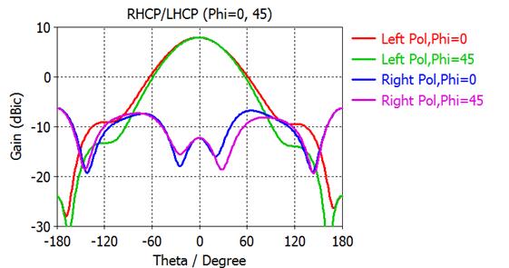
LHCP Pattern @2.25 Phi=45, Phi=0
RHCP/
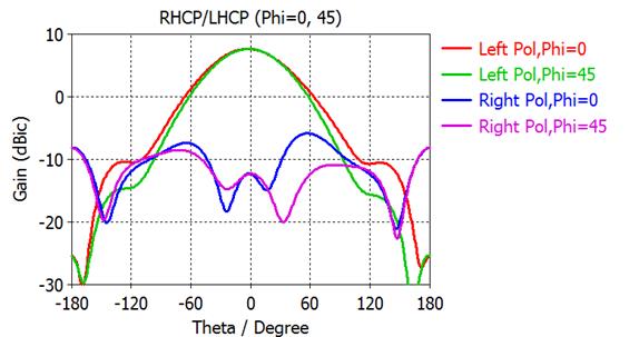
LHCP Pattern @2.5 Phi=45, Phi=0
RHCP/
LHCP Pattern @2.75 Phi=45, Phi=0
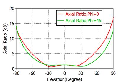
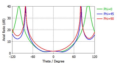
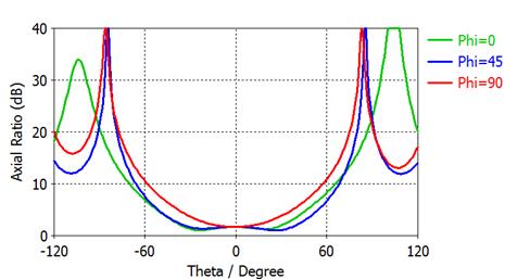
Axial
Ratio @ 2.15GHz:
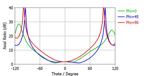
Axial
Ratio @ 2.25GHz:
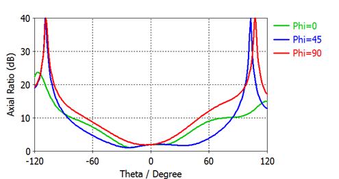
Axial
Ratio @ 2.5GHz:
Axial
Ratio @ 2.75GHz:
2. Design
2: 단일소자 design 2 사용