Antenna Design
Lab 10 - Inverted-L and inverted-F Antennas
I. Simulation
1. Monopole antenna
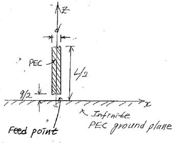
Monopole
dimensions:
Feeding:
Gap-fed with a discrete port with source impedance of 50 W
Design
frequency: f 0 = (1000 + PIN/1000)
MHz=1GHz
실습조교 PIN =
0000
Monopole axis:
in z direction
Reference
resonant dipole length: L = 0.45 λ =
0.45 ´ 300 = 135 mm
Monopole
end-to-ground plane distance: L/2 = 0.225 λ= 68
mm
Monopole
diameter: d = (L/2)/34 = 2.0 mm
Monopole feed gap: g/2 = d/2
= 1 mm
Monopole: PEC
Frequency range: 0.5f0 to
1.5f0
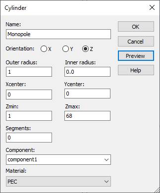
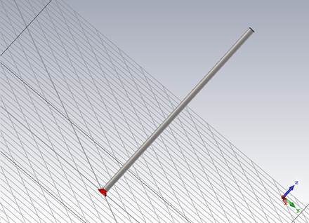
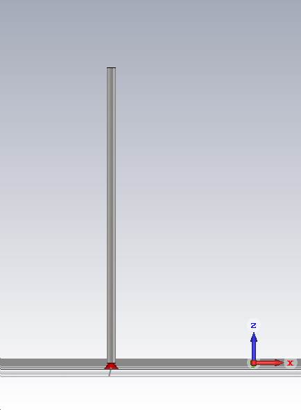
(1) Make the Monopole
Modeling, Cylinder 아이콘 선택, ESC 키, Name:
solid1, Orientation: Z
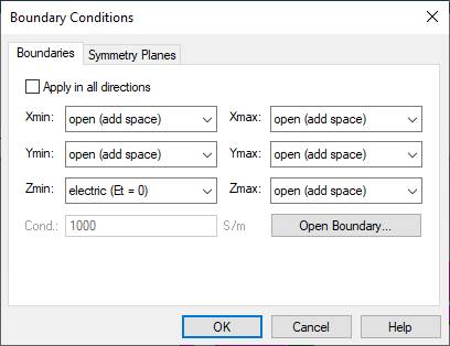
(2) Make an infinite PEC (Et = 0)
ground plane on the Zmin (z = 0) boundary box.
a) Boundaries configuration
Simulation, Boundaries, Boundary Conditions,
Zmin: choose the electric(Et=0), OK

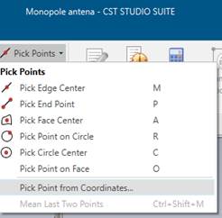
b) 포트설정
Modeling, Pick Points, Pick Face
Center, gap 한면에 마우스 위치후 더블클릭
Pick Points, Pick Face Center, gap 한면에 마우스 위치후 더블클릭
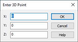
Modeling, Pick Points, Pick Point From
Coordinates
Enter 3D point, X:0, Y: 0, Z:0 OK
Simulation, Discrete Port
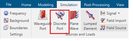
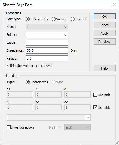
Simulation, Discrete Port, OK
Simulation,
Setup Solver
1) 시뮬레이션 설정
주파수 설정:
Simulation, Frequency, Min. frequency:
0.5, Max. frequency: 1.5
필드 모니터 설정:
Simulation, Field Monitor, E-field,
Frequency, Frequency:1, Apply
Simulation, Field Monitor, H-field and
Surface current, Frequency, Frequency:1, Apply
Simulation, Field Monitor, Far
field/RCS, Frequency, Frequency:1, Apply
Simulate
Simulation, Setup Solver, Start
1-1. Plot the antenna structure
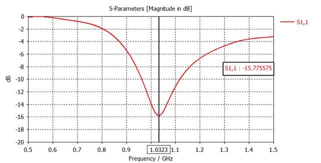
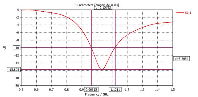
1-2. Plot |S11| (dB) at 0.5f0 to
1.5f0
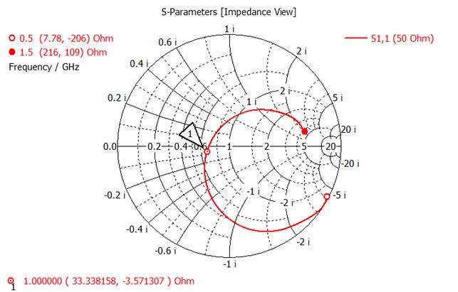
1-3. Plot the input impedance on the Smith chart.
1D Plot, Smith Chart
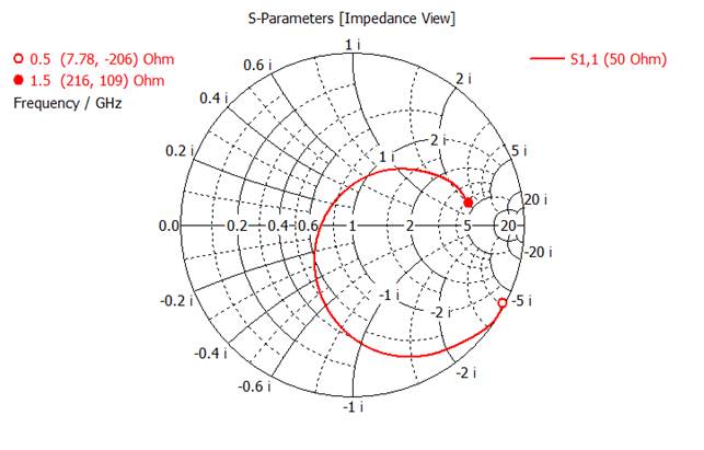
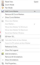
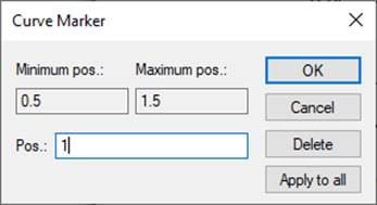
1-4. On the Smith chart, mark the
frequency f0 and find the input impedance Zin.
Add Curve marker and input frequency 1.0
Right-click, Add Marker, place the mouse
pointer on the curve and double-click
1-5. Plat 3D Gabs at f0.
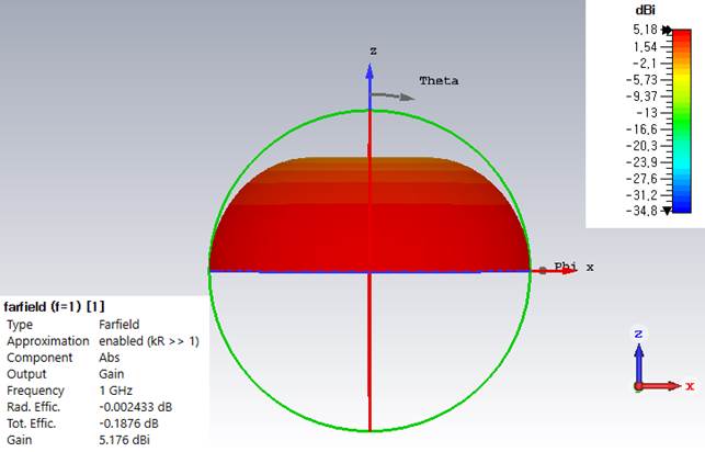
1-6. Find max(Gabs) at f0.
(Gabs)=5.176 dBi
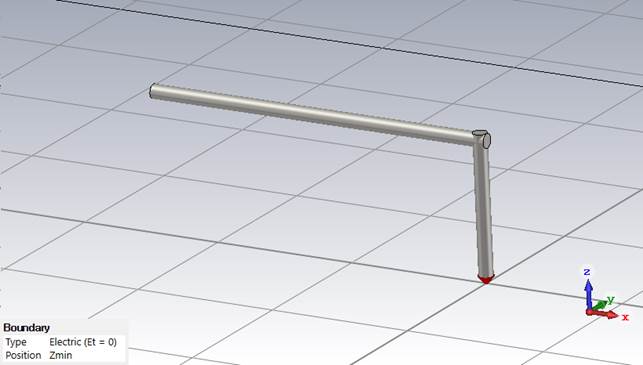
2. Inverted-L antenna (ILA)
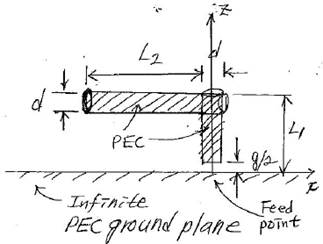
L1 = 0.3 (L/2), L2 =
0.7 (L/2), where L, g, and d are
defined in the above.
(1) Make the antenna geometry and plot it in
3D.
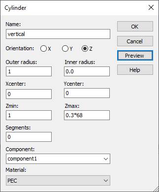
Vertical
Modeling, Cylinder 아이콘 선택, ESC 키, Name:
solid1, Orientation: Z
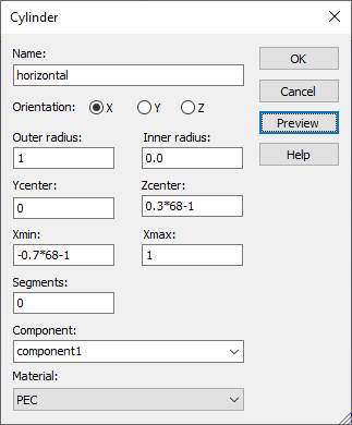
Horizontal
Modeling, Cylinder 아이콘 선택, ESC 키, Name: solid1,
Orientation: X

(2) Make an infinite PEC (Et = 0)
ground plane on the Zmin (z = 0) boundary box.
a) Boundaries configuration
Simulation, Boundaries, Boundary Conditions,
Zmin: choose the electric(Et=0), OK
(3) Make a discrete port.
Modeling, Pick Points, Pick Face
Center, select a face in the gap and double click.

Pick Points, Pick Face Center, gap 한면에 마우스 위치후 더블클릭
Modeling, Pick Points, Pick Point From
Coordinates
Enter 3D point, X:0, Y: 0, Z:0 OK

Simulation, Discrete Port
Simulation, Frequency, Min. frequency:
0.5, Max. frequency: 1.5
필드 모니터 설정:
Simulation, Field Monitor, E-field,
Frequency, Frequency:1, Apply
Simulation, Field Monitor, H-field and
Surface current, Frequency, Frequency:1, Apply
Simulation, Field Monitor, Far
field/RCS, Frequency, Frequency:1, Apply
Simulate
Simulation, Setup Solver, Start
2-1. Plot the antenna structure.

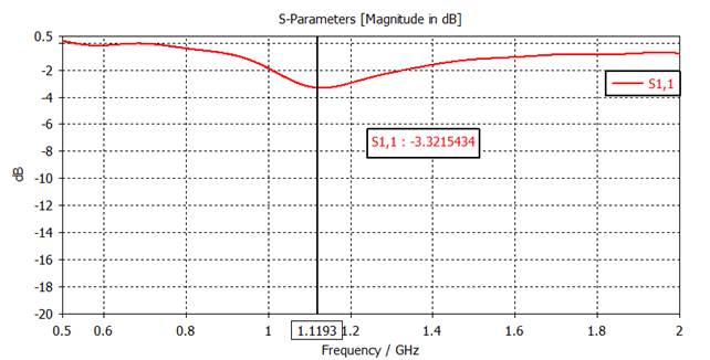
2-2. Plot |S11| (dB) at 0.5f0 to
2.0 f0.
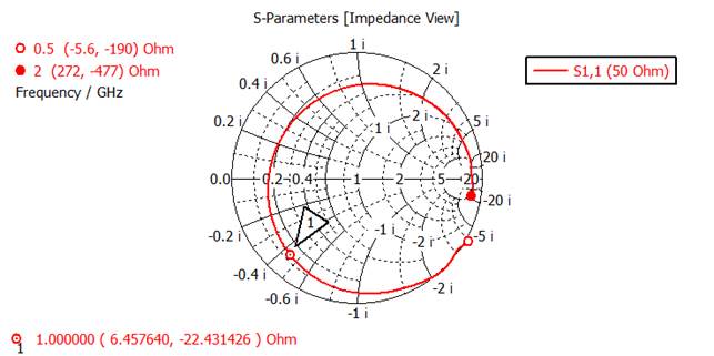
2-3. Plot the input impedance on the Smith
chart.
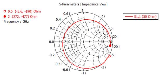 m
m
2-4. On the Smith chart, mark the frequency f0 and
find the input impedance Zin.
2-5. Plat 3D Gabs at f0.
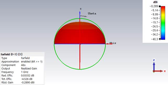
2-6. Find max(Gabs) at f0.
(Gabs)=-0.289 dBi
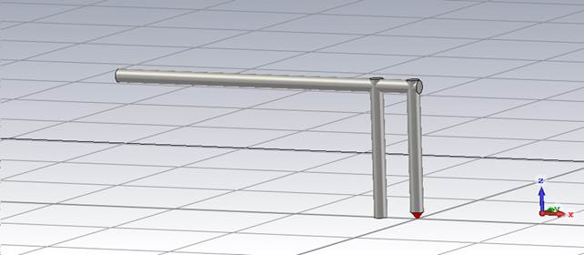
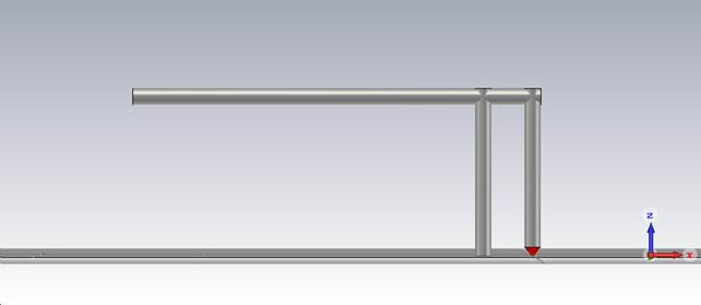
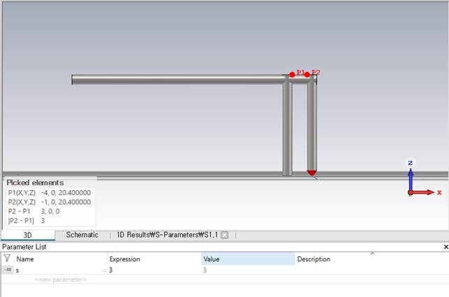
3. Inverted-F antenna (IFA)
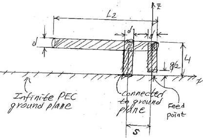
L1 = 0.3 (L/2), L2 =
0.7 (L/2), where L, g, and d are
defined in the above.
(1) Make the antenna geometry and plot it in
3D.
Vertical 1
Modeling, Cylinder 아이콘 선택, ESC 키, Name:
solid1, Orientation: Z

Horizontal
Modeling, Cylinder 아이콘 선택, ESC 키, Name:
solid1, Orientation: X
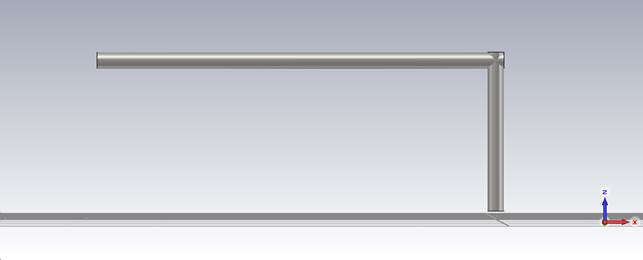
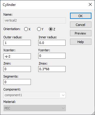
Vertical 2
Modeling, Cylinder 아이콘 선택, ESC 키, Name:
solid1, Orientation: Z
Ok
(2) Make an infinite PEC (Et = 0)
ground plane on the Zmin (z = 0) boundary box.
a) Boundaries configuration
Simulation, Boundaries, Boundary Conditions,
Zmin: choose the electric(Et=0), OK
(3) Make a discrete port.
Modeling, Pick Points, Pick Face
Center, select a face in the gap and double click.
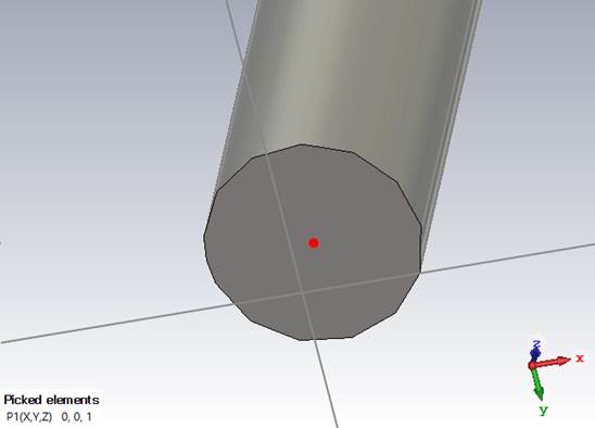
Pick Points, Pick Face Center, gap 한면에 마우스 위치후 더블클릭
Modeling, Pick Points, Pick Point From
Coordinates
Enter 3D point, X:0, Y: 0, Z:0 OK
Modeling, Pick Points, Pick Point From
Coordinates
Enter 3D point, X:0, Y: 0, Z:0 OK

Simulation, Discrete Port
Simulation, Frequency, Min. frequency:
0.5, Max. frequency: 2
필드 모니터 설정:
Simulation, Field Monitor, E-field,
Frequency, Frequency:1, Apply
Simulation, Field Monitor, H-field and
Surface current, Frequency, Frequency:1, Apply
Simulation, Field Monitor, Far
field/RCS, Frequency, Frequency:1, Apply
3-1. Plot the antenna structure.
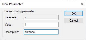
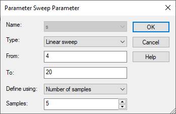
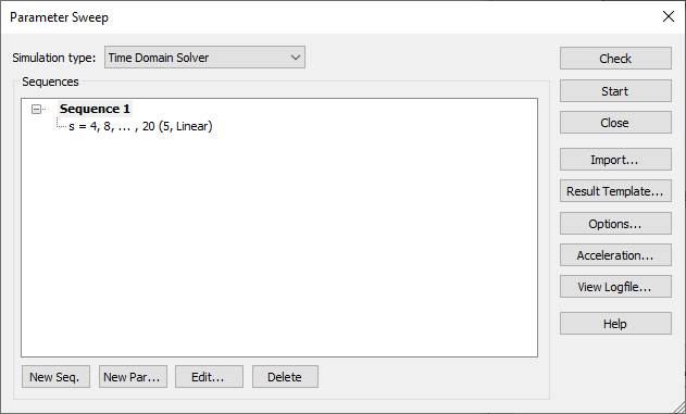
With all other dimensions fixed, change S to
the following values
S =
2d, 4d, 6d, 8d, and 10d
using the parameter sweep method in CST
Studio. If necessary, repeat the parameter sweep in smaller intervals for the
lowest value of min{|S11| (dB)}.
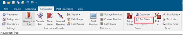
Simulation,
Setup Solver, Time Domain Solver Parameters, Par. Sweep,
New Sequence,
New Parameter, Parameter Sweep Parameter
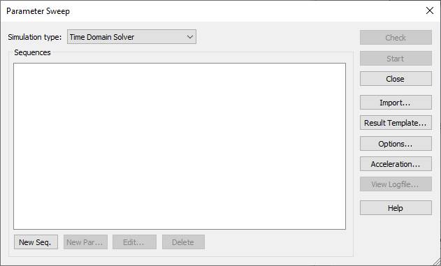
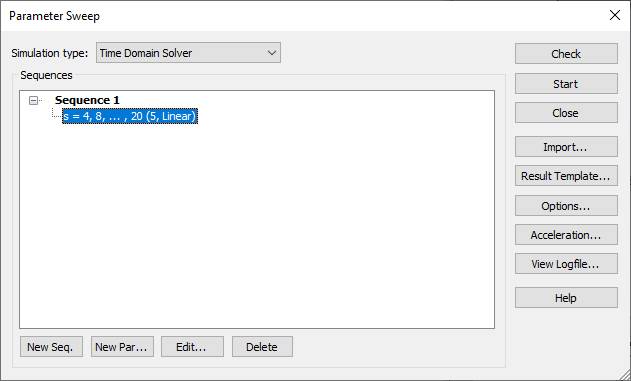
close
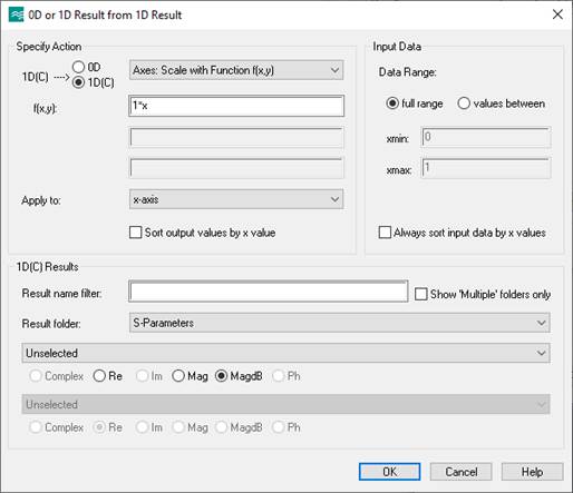
Post-Processing,
Result Templates Tools, General 1D, choose the 0D or 1D result from 1D Result
(Rescale, Derivation, etc)
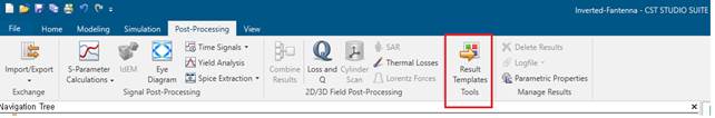
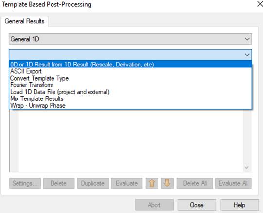
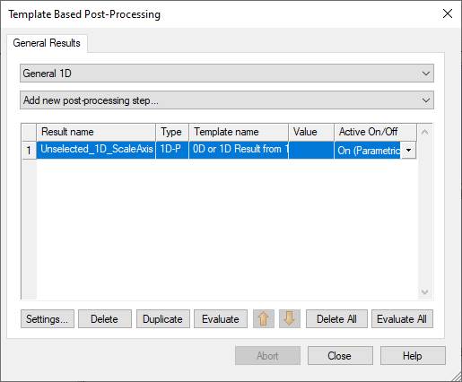
Evaluate All
Simulation,
Par.Sweep, Start
0D or 1D result.
1D Results,
S-Parameters, S1,1
RESULT TOOLS -
1D Plot, dB
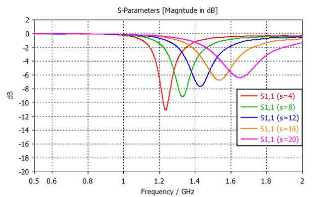
If necessary, repeat the parameter sweep in
smaller intervals for the lowest value of min{|S11| (dB)}.
S =
1, 2, 3, 4,5 and 6
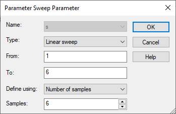
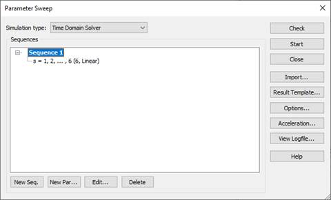
start

Now set S = Soptimum=3
and do the following
Change the S value (S=3)
Simulation, Field Monitor, Far
field/RCS, Frequency, Frequency:1.21, Apply
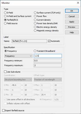
Simulate
Simulation, Setup Solver, Start
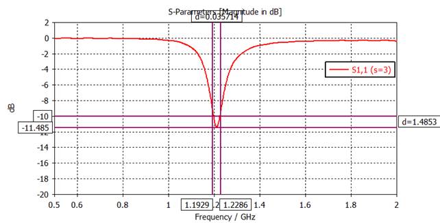
3-3. Plot
|S11| (dB) at 0.5f0 to 2.0 f0.

3-4.
Plot the input impedance on the Smith chart.
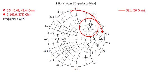
3-5.
On the Smith chart, mark the frequency f0 and find
the input impedance Zin
.

3-6.
Plat 3D Gabs at f0.
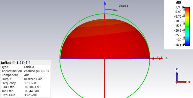
3-7.
Find max(Gabs) at f0.
(Gabs)= 3.928 dBi
Summarize your
simulation in the following table.
|
Antenna |
Frequency fC (GHz)
for minimum |S11| |
|S11| < -10 dB bandwidth (GHz) |
Rin, Xin at fC. |
Max (Gabs) at fC |
|
Monopole |
1.03 |
0.157 |
33,34-3,57 Ω |
5.176 dBi |
|
ILA |
1.12 |
- |
6.45-22.43 Ω |
-0.289 dBi |
|
IFA |
1.21 |
0.035 |
70.8+26.2 Ω |
3.92 dBi |